DDR TERMINATION REGULATOR
DESCRIPTION
The UTC UR5595 is a linear bus termination regulator
designed to meet JEDEC SSTL-2 and SSTL-3 (Stub Series
Terminated Logic) specifications for termination of DDR-SDRAM.
The device contains a high-speed operational amplifier to provide
excellent response to the load transients, and can deliver 1.5A
continuous current and transient peaks up to 3A in the application
as required for DDR-SDRAM termination.
With an independent VSENSE pin, the UR5595 can provide
superior load regulation. The UR5595 provides a VREF output as
the reference for the application of the chipset and DIMMs.
The output, VTT, is capable of sinking and sourcing current
while regulating the output voltage equal to VDDQ/2. The output
stage has been designed to maintain excellent load regulation and
with fast response time to minimum the transition preventing
shoot-through. The UTC UR5595 also incorporates two distinct
power rails that separates the analog circuitry (AVIN) from the
power output stage (PVIN). This power rail split can be utilized to
reduce the internal power dissipation. And this also permits UTC
UR5595 to provide a termination solution for DDRII SDRAM.
FEATURES
* Power regulating with driving and sinking capability
* Low output voltage offset
* No external resistors required
* Low external component count
* Linear topology
* Low cost and easy to use
* Thermal shutdown protection
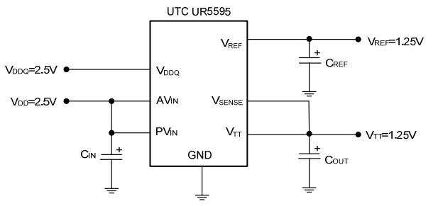
APPLICATION CIRCUIT
 |